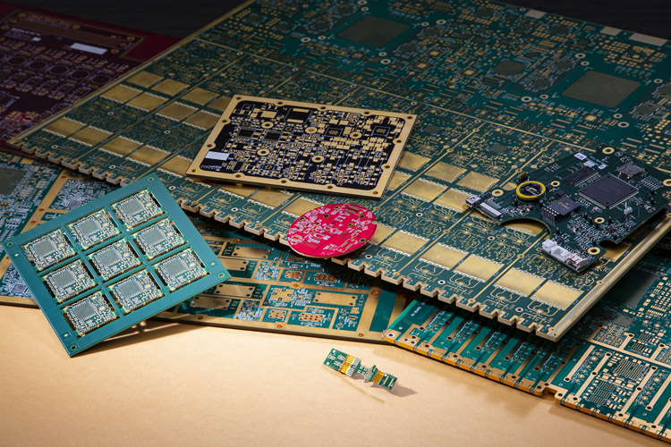

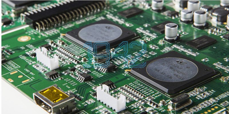
In SMT processing, the layout of components on the PCB board is very important, and it is also an important factor affecting the soldering quality. It should be designed according to the characteristics of SMT processing production equipment and chip processing technology. Different processes, such as reflow soldering and wave soldering, have different layouts of components on the PCB. During double-sided reflow soldering, there are also different requirements for the layout of side A and side B; selective wave soldering and traditional wave soldering also have different requirements. Today, Shenzhen 1942 Technology CO., LTD will share some information with you , welcome to discuss with us.
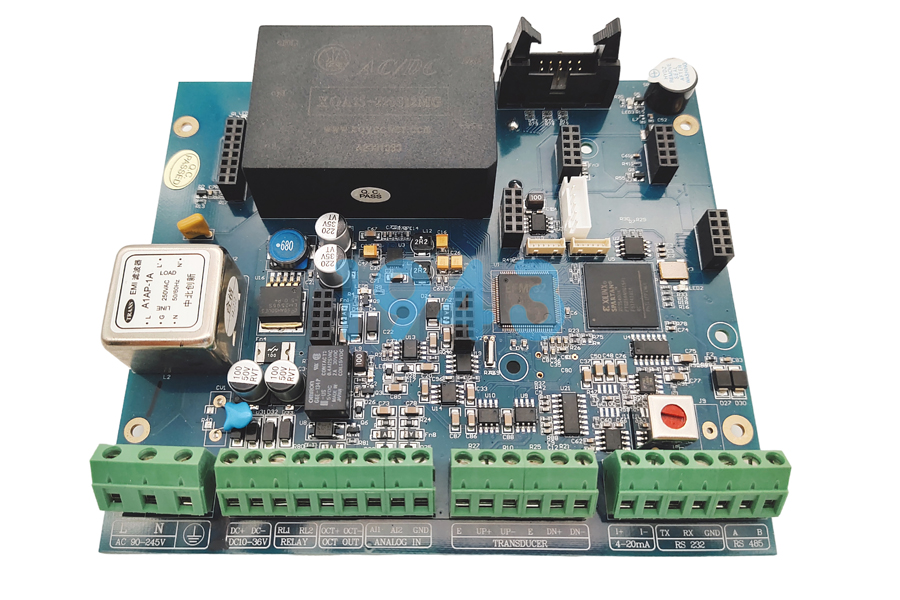
1. The distribution of components on the PCB board should be as uniform as possible. The heat capacity of large-volume components during reflow soldering is large, and excessive concentration will easily lead to low local temperature and lead to virtual soldering; at the same time, the uniform layout is also conducive to the balance of the center of gravity. It is not easy for components, metallized holes and pads to be damaged.
2. The arrangement direction of components on the PCB board, similar components are arranged in the same direction as possible, and the characteristic direction should be consistent, which is convenient for components to be welded and quality tested in SMT chip processing. For example, the positive electrode of the electrolytic capacitor, the positive electrode of the diode, the single-pin end of the triode, and the first pin of the integrated circuit are arranged in the same direction as possible.
3. The size of the heating head of the SMD rework equipment should be reserved around the large components.
4. SMT chip processing components with high heat generation should be kept as far away as possible from other components, generally placed in corners and ventilated positions in the chassis. The heating components should be supported by other leads or other supports (such as heat sinks can be added) to keep the heating components at a certain distance from the surface of the PCB, with a minimum distance of 2mm. The heating components are connected with the PCB board in the multi-layer board, and the metal pads are used in the design, and the SMT patch processing and welding are connected with solder, so that the heat is dissipated through the PCB board.
5. Temperature-sensitive components should be kept away from heating components. Such as triodes, integrated circuits, electrolytic capacitors and some plastic-shell components, etc., should be kept away from bridge stacks, high-power components, radiators and high-power resistors as much as possible.
6. The layout of components and parts that need to be adjusted or replaced frequently, such as potentiometers, adjustable inductance coils, variable capacitors, micro switches, fuses, buttons, plug-ins and other components, should be considered. Structural requirements, place it in a position for easy adjustment and replacement. If it is adjusted inside the machine, it should be placed on the printed circuit board where it is easy to adjust; if it is adjusted outside the machine, its position should be adapted to the position of the adjustment knob on the chassis panel to prevent conflicts between three-dimensional space and two-dimensional space. For example, the panel opening of the toggle switch and the vacant position of the switch on the printed circuit board should match.
7. Fixing holes should be provided near the terminals, plug-in parts, the center of the long string terminals and the parts that are often subjected to force, and there should be a corresponding space around the fixing holes to prevent deformation due to thermal expansion. For example, the thermal expansion of the long series of terminals is more serious than that of the printed circuit board, and it is prone to warping during wave soldering.
8. Some components and parts (such as transformers, electrolytic capacitors, varistors, bridge stacks, radiators, etc.) that require secondary processing with large tolerances and low precision, and other components The interval is increased by a certain margin on the basis of the original setting.
9. It is recommended to increase the margin of electrolytic capacitors, varistors, bridge stacks, polyester capacitors, etc., not less than 1mm, and transformers, radiators and resistances exceeding 5W (including 5W) should not be less than 3mm.
10. Electrolytic capacitors should not touch heating components, such as high-power resistors, thermistors, transformers, radiators, etc. The minimum distance between the electrolytic capacitor and the radiator is 10mm, and the minimum distance between other components and the radiator is 20mm.
11. Do not place stress-sensitive components on the corners, edges, or near connectors, mounting holes, slots, cuts, gaps, and corners of the printed circuit board. These positions are high stress on the printed circuit board. It is easy to cause cracks or cracks in solder joints and components.
12. The component layout should meet the process requirements and spacing requirements of SMT chip processing, reflow soldering, and wave soldering. Reduces shadowing effects during wave soldering.
13. The positioning holes of the PCB board and the positions to be occupied by the fixing brackets should be reserved.
14. In the design of large-area PCB, in order to prevent the PCB from bending and deforming during reflow soldering and wave soldering, a 5-10mm wide gap should be left in the middle of the printed circuit board, and no components (can be routed) should be placed for use. To prevent the PCB board from bending and deforming during the soldering process.
15. The layout of components on the PCB board should consider the reflow soldering process. The board entry direction, the heat capacity of the components, and the long axis of the SMD components should be parallel to the reflow soldering transfer direction, and the CHIP components should be perpendicular to the reflow soldering transfer direction.
16. The minimum installation spacing of components must meet the manufacturability, testability and maintainability of SMT chip processing.
 2026-05-30