

Last time henzhen 1942 Technology Co., LTD shared some views about PCB, now we are going on
4.PCB Break Away Tab
The processing flow of PCBA needs to be transmitted by the transmission tracks of various machines and equipment and the tracks between the equipment. In order to ensure that the PCB can be fixed, a size of 5mm is generally reserved at the outer edge of the PCB to facilitate the clamping of the equipment, and devices are not allowed to be mounted in the process edge. When it is impossible to reserve, the process edge must be added.
For some products whose plug-ins need to pass wave soldering oven, a size of 3mm shall be reserved on the short side to block the solder paste.
5.PCB Datum point (Mark)
The datum point, also known as mark, provides a common reference point for all steps in the SMT assembly process, ensuring that each device used in the assembly can precisely locate the pattern of the circuit. Therefore, the Mark is very important for the machining of the PCBA. The Mark is generally divided into the whole board Mark, the panel Mark, the local identification Mark (the pin spacing ≤ 0.5mm), generally stipulating that the marking point in the center of the Mark is metal copper foil, with a diameter of 1.0mm, the diameter of the surrounding empty comparison area is 3mm, and the color contrast between the metal copper foil and the surrounding open area is obvious. Silk screen printing, pads or V-Cuts are not allowed in the Φ3mm range.
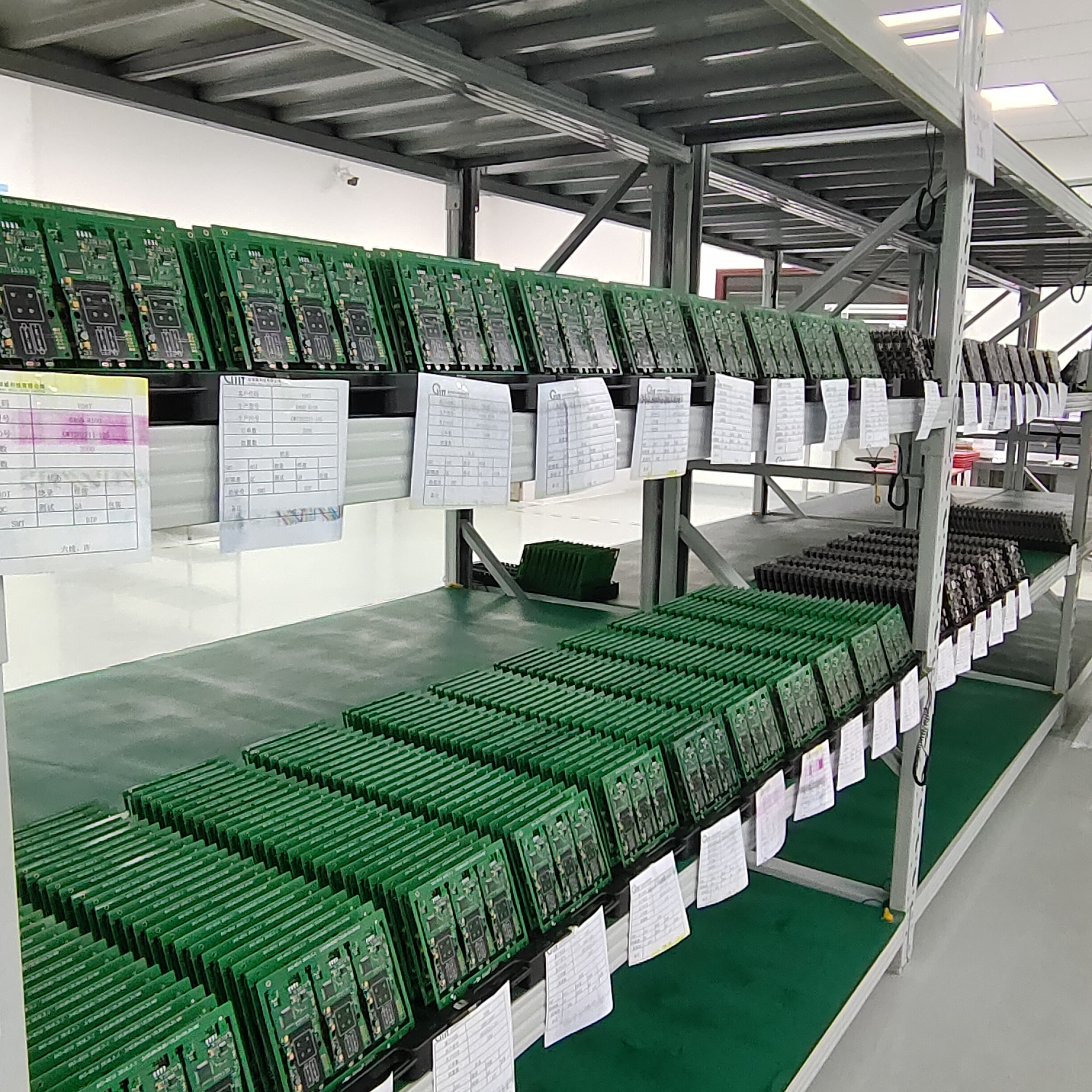
6.Imposition design
General principle: When the size of the single PCB is less than 50mm×50mm, it must be made into a panel. It can be converted to a size that meets production requirements for plugin and soldering, and improving production efficiency and equipment utilization. However, it should be noted that the size of the panel cannot be too large, and it must meet the requirements of PCBA processing equipment. V-shaped slot, stamp holes or punching slot can be used between the panels;
7. Can withstand solvent washing.
When we assemble components, due to the flux in the solder paste, its solder joints are easy to become dirty, it usually need to use clean solvents such as washing agent for cleaning. Therefore, the PCB should be able to withstand the washing of solvents, and the surface of the PCBA should not appear bubbles and whitish some undesirable phenomena.
#Shenzhen 1942 #PCBA #SMT factory #PCB design #PCB layout #double layer PCB #PCB assembly #PCB
 2024-06-03