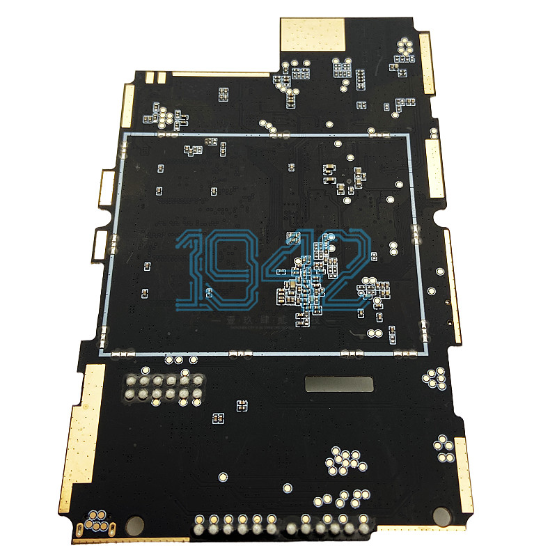
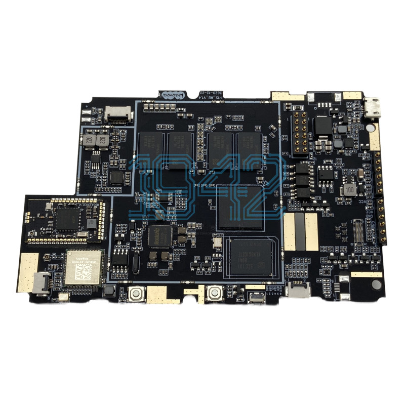
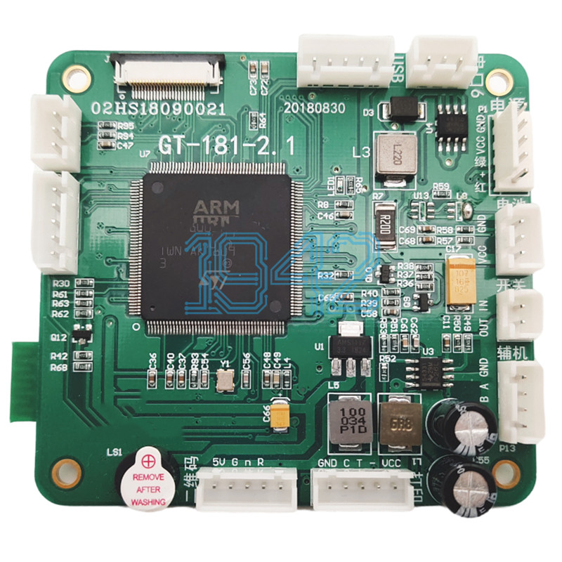
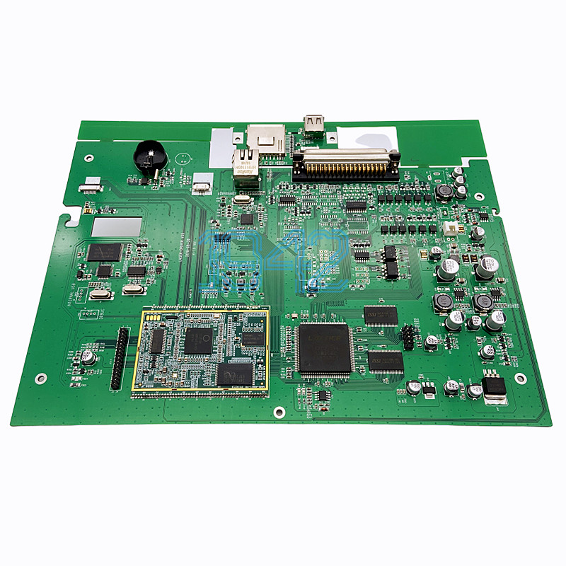
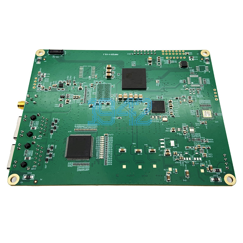
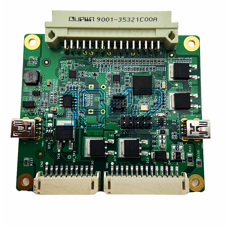
Point:362
Components type:91
PCB size: 132*97mm
Minimum package size of resistance capacitance sensing: 0402
Minimum device pin spacing:0.5
Welding mode:Reflow soldering for double side + Wave soldering.
Manufacturing process: PCB producing + components procurement + assembly
Shenzhen 1943 Technology Co., LTD. provides end-to-end printed circuit board fabrication and assembly solutions specialized for smart home control systems. As modern smart home devices demand higher component density, lower power consumption, and multi-protocol wireless connectivity (such as Wi-Fi, Bluetooth, Zigbee, and Thread), our engineering and production facilities are equipped to deliver highly stable PCBs engineered for continuous, long-term operation.
Bringing a new smart home device to market requires a precise and efficient transition from CAD design to physical hardware. To support hardware startups and established OEMs alike, Shenzhen 1943 Technology Co., LTD. offers comprehensive NPI Services (New Product Introduction). Our PCBA manufacturing one-stop NPI service is structured to streamline early-stage development, mitigate design risks, and accelerate your time-to-market:
Design for Manufacturing & Assembly (DFM/DFA): Rigorous engineering reviews of Gerber files, BOMs, and centroid data to identify potential footprint mismatches, solder bridging risks, or component clearance issues before production begins.
Component Sourcing & AVL Management: Procurement of active and passive components through authorized global distributors, ensuring full traceability and offering reliable second-source options for critical ICs.
Rapid Prototyping: Flexible, dedicated SMT lines configured to handle small-batch prototype runs quickly, allowing physical validation of your circuitry.
Process Optimization: Detailed documentation of assembly profiles, thermal profiling for reflow ovens, and fixture design to establish a repeatable baseline for future volume production.

Our production facility supports complex layouts and high-density packaging typical of IoT and smart home controller boards:
PCB Fabrication: Multilayer boards up to 20 layers, Rigid-Flex PCBs for space-constrained enclosures, High-Density Interconnect (HDI) boards with laser microvias, and impedance-controlled RF stackups.
Substrate Materials: Standard FR-4, High-TG FR-4 (for high-temperature environments), halogen-free materials, and aluminum-clad/MCPCB for smart LED lighting control.
Surface Mount Technology (SMT): High-speed placement of components down to 01005 package sizes, fine-pitch QFNs, and BGAs down to a 0.35mm pitch.
Through-Hole Technology (THT): Automated wave soldering and selective soldering for heavy-duty relays, terminals, and power connectors.
We execute systematic inspection protocols to guarantee the reliability of smart home control systems:
Inspection: 3D Solder Paste Inspection (SPI), Automated Optical Inspection (AOI), and non-destructive X-Ray Inspection for BGA solder joint integrity.
Functional Testing (FCT): Custom testing jig development to run firmware, verify peripheral communication ports, test RF output power, and validate sensor interfaces.
Standards Compliance: Assembly in accordance with IPC-A-610 Class 2 or Class 3 guidelines. All materials are RoHS/REACH compliant, and production facilities operate under ISO 9001:2015 quality management systems.
Let the products quickly and stably realize marketization and become the global electronic intelligence innovation enabler