Industrial control

PCBA Manufacturing & PCB Design for Laser Marking Machines | PCBA NPI Services

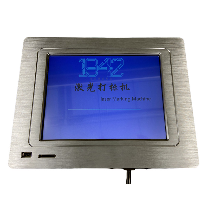
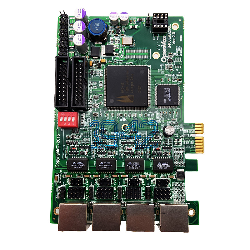
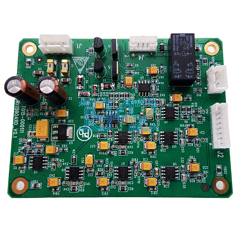
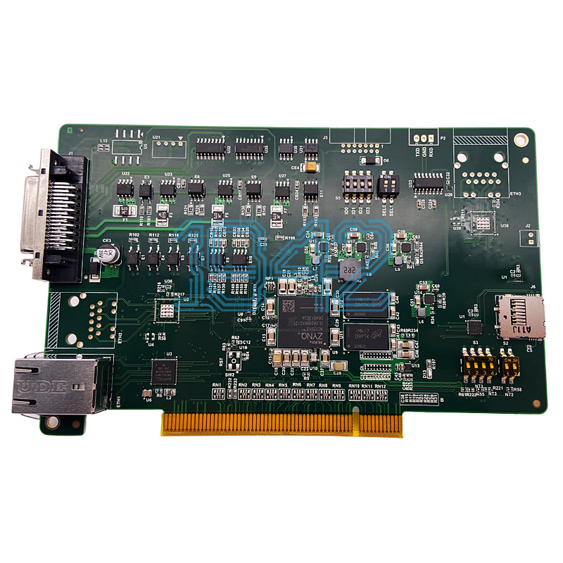
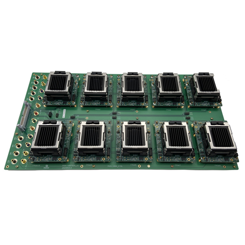
Shenzhen 1943 Technology provides PCB design, PCBA manufacturing, and PCBA NPI services for laser marking machines and industrial electronics, including process validation, material evaluation, reliability testing, and mass production preparation.

Point:472

Components type:124

PCB size: 256mm*184mm

Minimum package size of resistance capacitance sensing: 0402

Minimum device pin spacing:0.5

Welding mode:Reflow soldering for double side + Wave soldering.

Manufacturing process: PCB producing + components procurement + assembly

PCBA Manufacturing and PCB Design for Laser Marking Machines, along with PCBA NPI Services

Shenzhen 1943 Technology Co., Ltd. provides specialized PCBA manufacturing, PCB design support, and New Product Introduction (NPI) services tailored to laser marking machines and related industrial equipment. Our work supports the full transition from engineering prototypes to stable production volumes in demanding applications.

PCB Design and PCBA Manufacturing Capabilities

We handle PCB design considerations specific to laser marking systems, which often require precise control circuits, stable power delivery, thermal management for high-duty cycles, and reliable interfaces for galvanometer drivers, laser sources, and motion control. Our engineering team reviews layouts for signal integrity, impedance control where needed, and manufacturability to align with the mechanical and environmental demands of these machines.

In manufacturing, we support rigid FR-4 boards, metal-core options for heat dissipation, and multilayer configurations typical in industrial controls. Our SMT lines accommodate component packages down to 0201, with placement accuracy suitable for dense assemblies. Processes include automated solder paste printing, high-speed placement, reflow, and selective or wave soldering for through-hole components. We perform AOI, X-ray inspection for BGAs or hidden joints, and functional testing to verify performance under load.

Full PCBA services cover component sourcing, PCB fabrication, SMT and DIP assembly, testing, final integration, and packaging. For laser marking equipment, this includes attention to vibration resistance, electrical noise immunity, and long-term operational stability in factory settings. We manage production for prototypes, pilot runs, and medium-to-small batch volumes with consistent process controls.

PCBA One-Stop NPI Services

PCBA NPI Services: Bridging Development to Production

NPI serves as the essential step when moving from research and development to volume manufacturing. It establishes clear standards and verifies that the product can be built reliably and repeatedly. At 1943 Technology, our dedicated NPI approach focuses on four main verification areas that directly address common risks in electronics for industrial machines like laser markers.

First, we validate the manufacturing process across the full flow: PCB fabrication, SMT placement, DIP insertion, in-circuit and functional testing, mechanical assembly, packaging, and protective measures such as conformal coating or potting where required for harsh environments. This confirms process parameters like stencil design, reflow profiles, and handling steps produce consistent results before scaling.

Second, we examine material selection and supply chain stability. This includes reviewing the bill of materials (BOM) for component availability, lifecycle status, alternatives for long-lead or obsolete parts, and sourcing from reliable channels. For laser marking systems, this ensures critical components like drivers or sensors maintain performance without unexpected disruptions.

Third, product reliability receives focused attention through first-article inspection, pilot builds, and targeted testing. We assess thermal performance, electrical characteristics, and mechanical integrity to identify potential failure points early, helping achieve the durability expected in continuous industrial use.

Fourth, we evaluate the overall project timeline against market requirements. By identifying and resolving issues during NPI, we help align development, validation, and ramp-up phases to support timely launch without compromising quality or cost targets.

Our NPI process typically includes DFM/DFT reviews, process capability studies, documentation of work instructions and control plans, and yield analysis. This structured verification reduces iteration loops and supports a smoother handoff to ongoing production. Facilities feature 5000㎡ of space with 7 SMT lines, ESD controls, and ISO 9001 / ISO 13485 certifications, allowing us to handle the full chain under one roof.

Customers in industrial automation and related fields work with us because the combination of targeted PCB design input, capable manufacturing, and methodical NPI helps turn functional designs into field-ready products with fewer surprises. We maintain traceability, version control, and open communication throughout to keep projects on track.


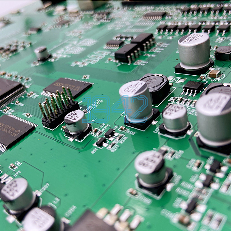
The total number of front and back surface mount components is 472

The amount types are 124

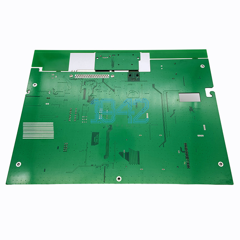
The outer diameter of PCB is 256mm*184mm

The minimum package size of surface mounted components is 0402

The minimum pin spacing of surface mount components is 0.5mm

Components are soldered by double-sided reflow soldering machine & wave soldering oven


Soldering Details 
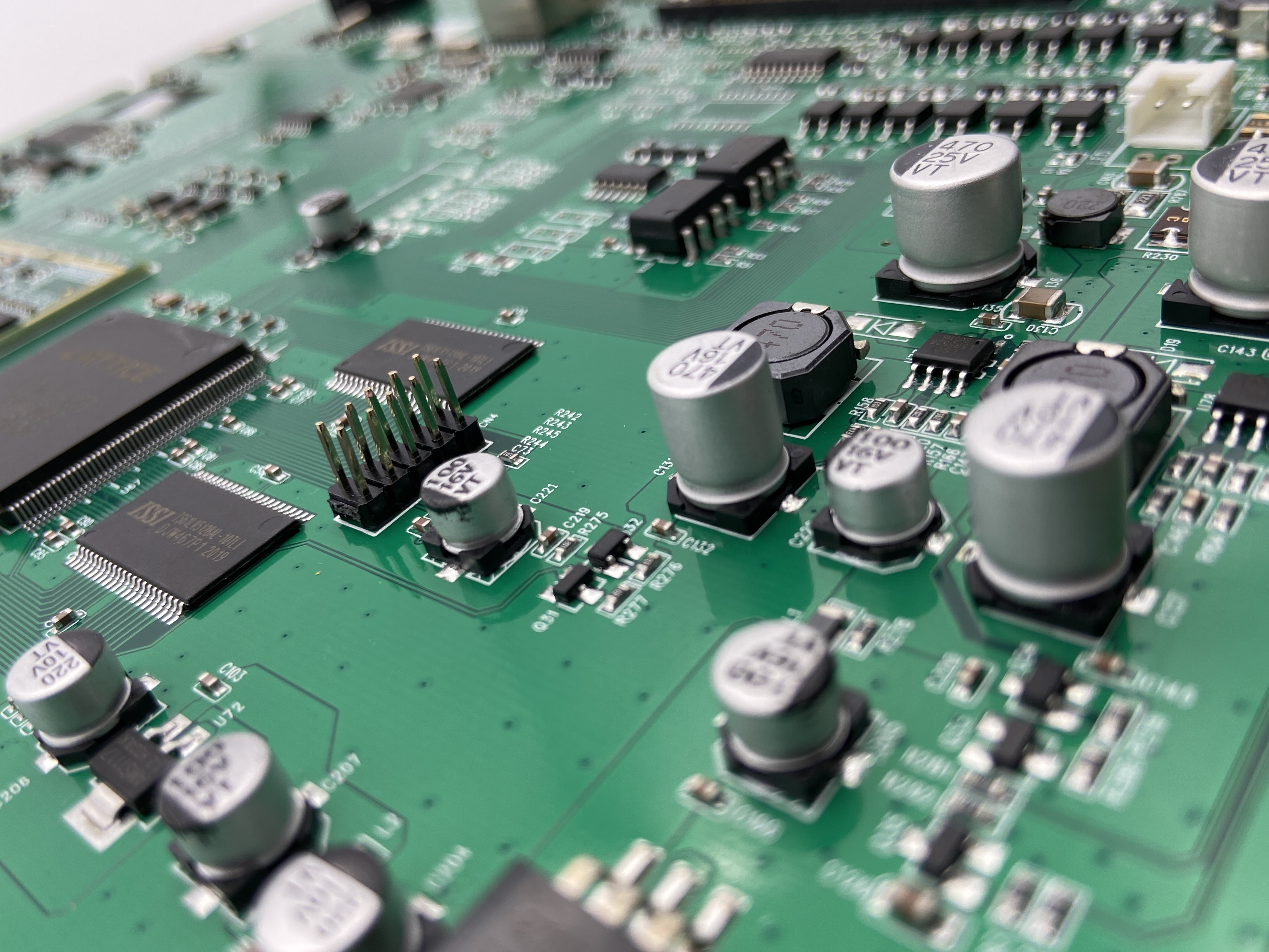
laser machine PCBA PCB manufacturer SMT factory PCBs shenzhen


Module Mounting

PCB module, SMT components, DIP , China SMT factory

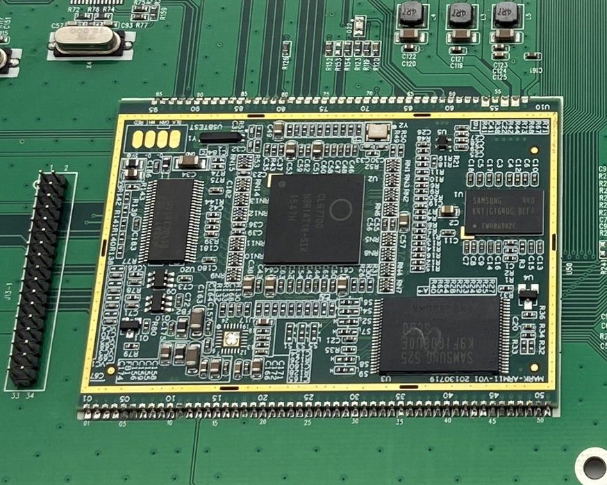
The production technical difficulty of this product is mainly the mounting of modules. It is necessary to ensure that the mounting height of modules is consistent . Furthermore, this module is very easy to be mountedwith false soldering.


Main chip mounting
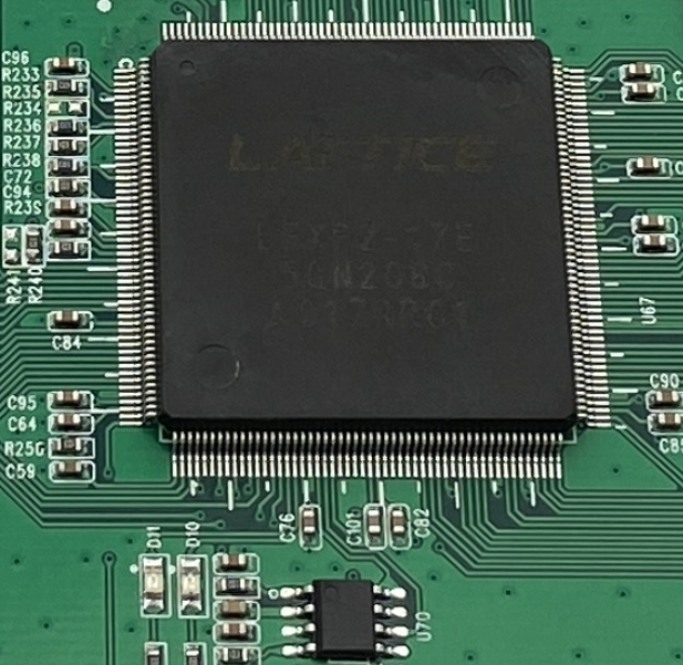
Laser marking machine|PCBs- circuit board manufacturing-PCB design_1943 Shenzhen

The number of pins is large and the spacing is small. The surface mounting process should be very high. At the same time, pay attention to the cleaning of PCBs board.