Industrial control

Laser marking machine|PCBA one stop service from PCB design to PCBs

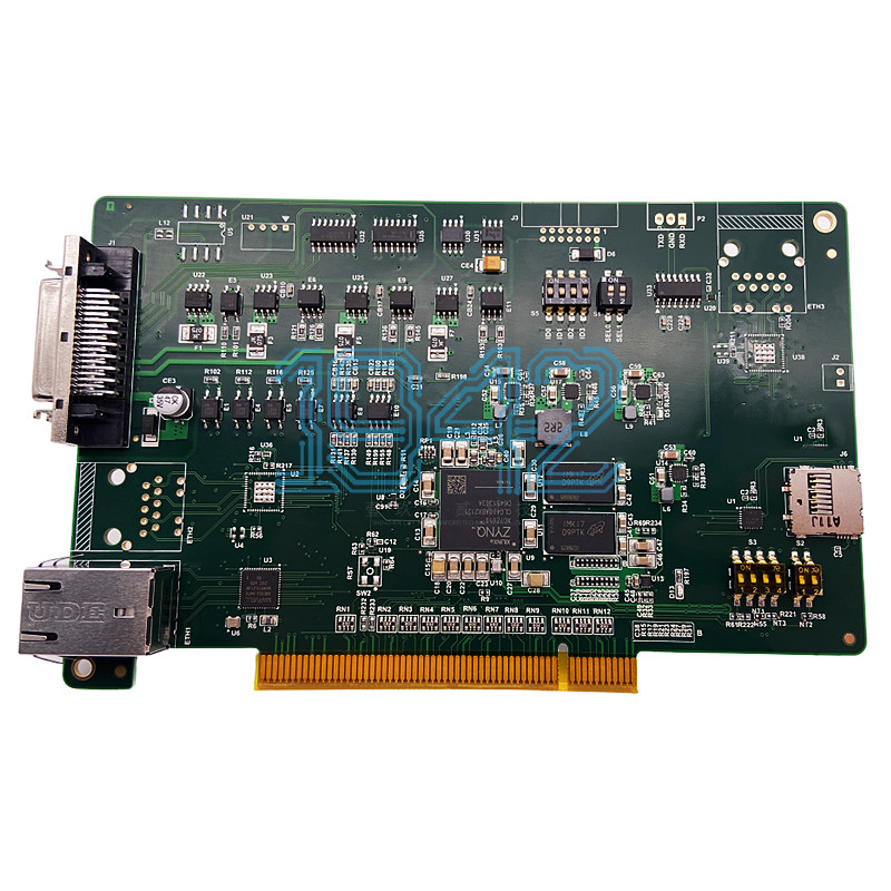
Shenzhen 1943 Technology offers PCBA manufacturing, PCB design support, and NPI services for laser marking machines. Process validation, material sourcing, reliability testing, and timeline alignment from prototype to production.

Point:433

Components type:125

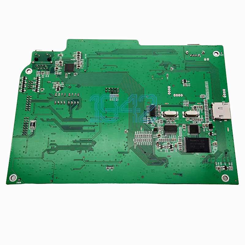
PCB size: 186mm*147mm

Minimum package size of resistance capacitance sensing: 0402

Minimum device pin spacing:0.5mm

Welding mode:Reflow soldering for double side + Wave soldering.

Manufacturing process: PCB producing + components procurement + assembly

Shenzhen 1943 Technology Co., LTD. provides end-to-end PCBA manufacturing, custom PCB design, and specialized New Product Introduction (NPI) services for laser marking machines and industrial control systems. We support clients from early-stage design optimization through trial production to full-scale manufacturing, ensuring high reliability, thermal stability, and strict quality control for precision laser equipment.


Core Services

1. Custom PCB Design & Layout

  • Laser Control Integration: Specialized board layouts for laser power control, galvo scanner drivers, high-speed signal processing, and system safety interlocks.
  • DFM/DFA Optimization: Early-stage Design for Manufacturability and Assembly checks to minimize redesign cycles and reduce unit costs.
  • Thermal Management: Engineered copper layouts and heavy-copper stackups designed to handle thermal stress in continuous laser operation environments.

2. Specialized PCBA Manufacturing

  • Surface Mount Technology (SMT): Precision placement for high-density components, fine-pitch ICs, BGA, and power modules.
  • Through-Hole Technology (DIP): Manual and selective soldering for heavy connectors, high-power relays, and structural components.
  • Full Box Build & System Integration: Complete assembly, cable harness integration, enclosure mounting, and protective coating (conformal coating/potting).

NPI (New Product Introduction) Services

NPI is a crucial bridge between initial engineering design and full mass production. At 1943 Technology, our NPI process establishes standardized operational benchmarks across four core evaluation stages:

  1. Process & Manufacturing Validation We rigorously verify every production stage—including SMT, DIP, functional testing, final assembly, packaging, and conformal protection—to ensure process capability, yield rate, and repeatability before mass production.
  2. Component Selection & Supply Chain Reliability We evaluate component selection for long-term availability, lifecycle status, and operational parameters, while confirming supply chain stability to mitigate lead-time risks and single-source dependencies.
  3. Product Reliability Verification Through environmental stress testing, thermal loading evaluation, and electrical functional verification, we ensure the PCBA performs consistently under continuous laser marking operations.
  4. Project Timeline & Lead Time Alignment We streamline pilot runs and validation steps to control project schedules, ensuring product time-to-market aligns directly with commercial planning and market requirements.

Quality Control & Testing

  • Inspection Systems: Automated Optical Inspection (AOI), X-ray inspection for BGA/QFN solder joints, and 3D SPI (Solder Paste Inspection).
  • Functional & Electrical Testing: In-Circuit Testing (ICT), custom functional testing (FCT), and burn-in testing under operational power conditions.
  • Traceability: Component lot tracking and process logging throughout the assembly pipeline.

PCBA One-Stop NPI Services


The total number of front and back surface mount components is 433

The amount types are 125

The outer diameter of PCB is 186mm*147mm

The minimum package size of surface mounted components is 0402

The minimum pin spacing of surface mount components is 0.5mm

Components are soldered by double-sided reflow soldering machine & wave soldering oven 

Module mounting
Laser marking machine|PCBA one stop service from PCB design to PCBs

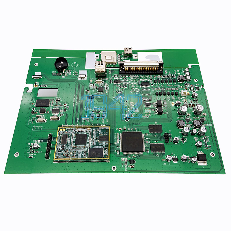
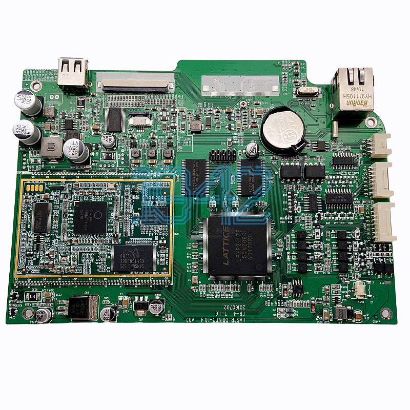
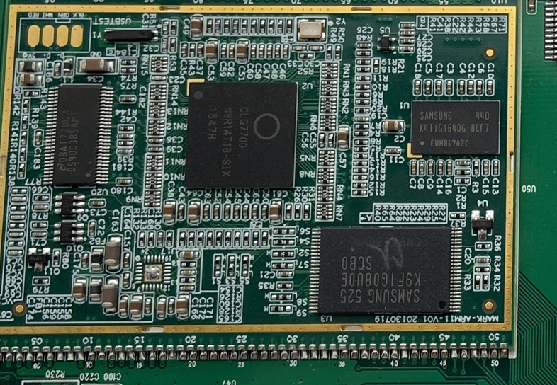
The production technical difficulty of this PCBs is mainly the mounting of modules. It is necessary to ensure that the mounting height of modules is consistent . Furthermore, this module is very easy to be mountedwith false soldering.


Main chip mounting
Laser marking machine|PCBA one stop service from PCB design to PCBs

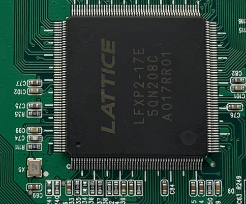
The number of pins is large and the spacing is small. The surface mounting process should be very high. At the same time, pay attention to the cleaning of PCBs board
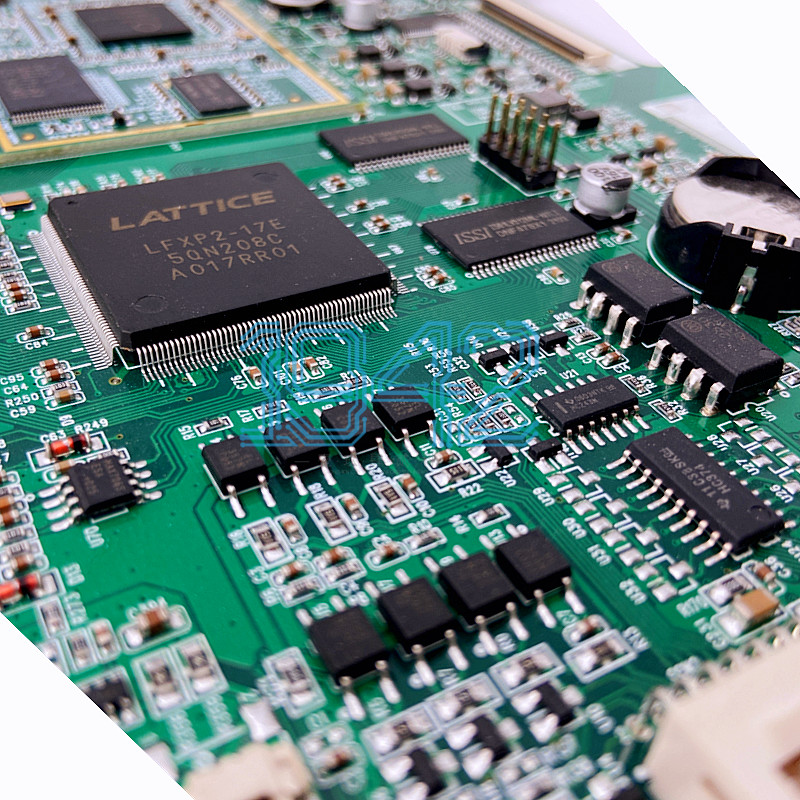
Laser marking machine|PCBA one stop service from PCB design to PCBs

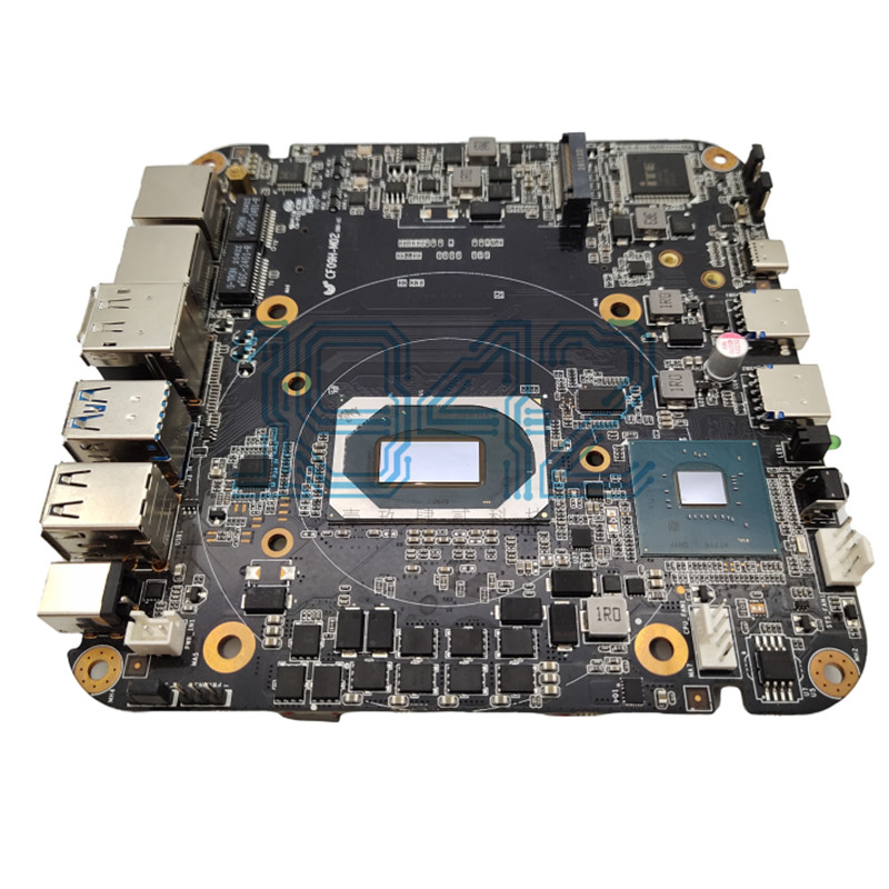
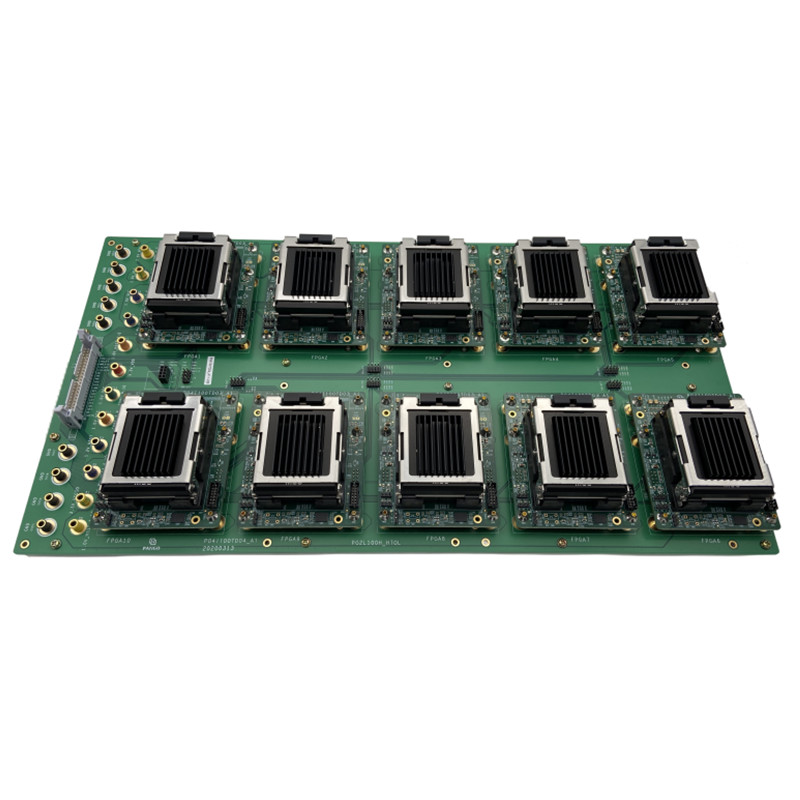
The  design and mounting of this Laser marking circuit board are very difficult, because the PCB size is small, but the design is very complex, there are many kinds of materials, and there is a large module, which reflects a high design level and mounting technology