

The soldering reliability of SMT processing components mainly depends on the length of the pads on the PCB surface rather than the width. The length B of the pad is equal to the length T of the terminal (or pin) plus the extended length b1 of the inside (pad) of the terminal (or lead), plus the outside (pad) of the terminal (or lead) The length b2 of , that is, B=T+b1+b2. b1=0.05~0.6mm, it should not only help to form a good meniscus profile when the solder is melted, but also avoid the bridging phenomenon of the solder and take into account the placement deviation of components; b2=0.25~1.25mm, mainly based on The solder joints that ensure the best meniscus profile are suitable for the pad peeling resistance of SOIC, QFP and other components. As shown below (ideal SMT processing solder joint shape and PCB surface pad)
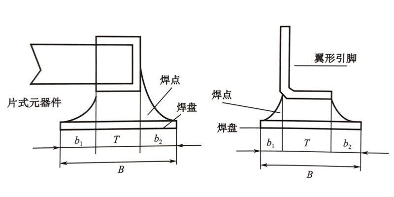
(ideal SMT patch processing solder joint shape and PCB surface pad)
1. The width of the PCB pad is less than or equal to the width of the solder end (pin). The corrections for the width are 0, ±0.1mm and ±0.2mm respectively; the width of the pad determines the position during the application of solder paste and reflow soldering and prevents the rotation or offset of SMT components.
2. The spacing of the PCB pads controls the horizontal movement of components during the solder paste application/reflow process.
3. No through-holes are allowed in the PCB pad and its edges; the distance between the through-hole and the edges on both sides of the pad should be greater than 0.6mm; if the through-hole pad needs to be interconnected with the pad, it can be less than the width of the pad by 1 /2 connection, such as 0.2 ~ 0.4mm to be interconnected to avoid various soldering problems caused by solder loss.
4. Characters and graphics are not allowed in the pads used for welding and testing, and the characters and graphics should be 0.5mm away from the pads.
5. The width of the connection between PCB pads, between through holes and pads, and between pads and large-area grounding or shielding copper foil should be less than or equal to 1/2 of the pad width, generally 0.2~ 0.4mm; if separated by solder mask, the width of the connection can be equal to the width of the pad.
6. For the same SMT processing component, all the pads used symmetrically, such as chip resistors, capacitors, SOIC, QFP, etc., should be designed to maintain their overall symmetry, that is, the shape and size of the pads are completely Consistent.
7. No through-holes are allowed between the pads of components such as chip resistors and chip capacitors without external leads (except those blocked by solder mask) to ensure the quality of cleaning.
8. For multi-lead SMT processing components such as SOIC and QFP, direct short-circuiting between the pin pads is not allowed. The interconnect lines should be drawn from the pads and then short-circuited to prevent displacement or bridging. Reduce the interconnection lines crossing between the pads, and the interconnection lines crossing between the pads must be protected with a solder mask.
9. For multi-lead components with a spacing below 0.65mm, a bare copper reference mark should be added on or near the pad pattern for optical calibration.
10. The PCB pad cannot be used as a detection point, and a dedicated test pad should be designed. The test pads should be arranged on the same side of the printed circuit board.
11. When designing with a computer, the selected network size must match it to ensure that the graphics (pads, fiducial marks, interconnect lines, etc.) all fall on the network points.
12. For multi-pin and fine-pitch components, the overall class error must be controlled within ±0.0127mm in the pad design.
13. A large pad should not be used between two components.
14. The pads and the PCB board must be inspected and qualified after the SMT processing and manufacturing, before they can be used.
15. The non-soldering area must be strictly welded.
16. The leadless chip chip processing components must be directly mounted on the pads, that is, they are not allowed to be designed to be stacked, not designed to be bridged between binding posts or correctly installed components, and side mounting is not allowed. .
welcome to visit Shenzhen 1942 Technology Co., Ltd.
 2026-04-30