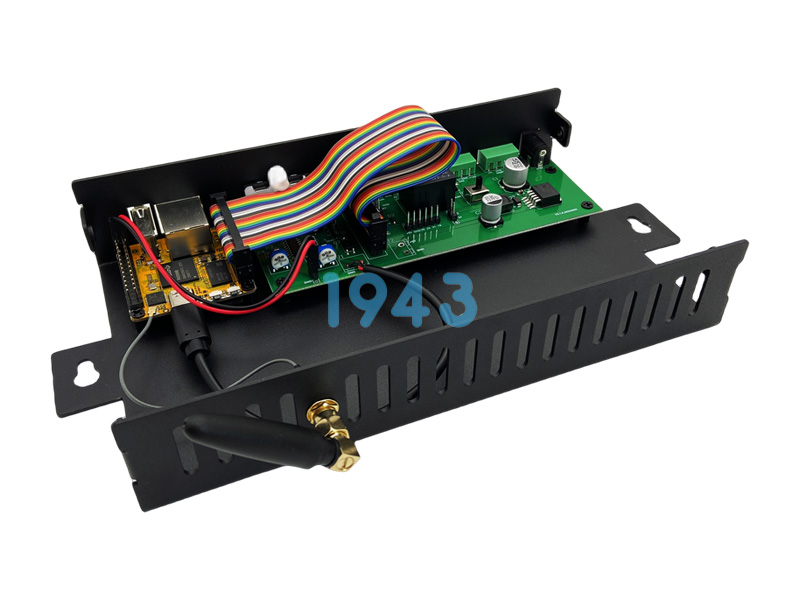

Small-Batch PCBA NPI: Scaling High-Mix Low-Volume Production
The Specific Technical Demands of HMLV NPI
For engineering-centric companies producing complex equipment in industrial, medical, and networking sectors, market success depends on rapid iteration and high product diversity, rather than mass unit production. Navigating the New Product Introduction (NPI) phase for High-Mix Low-Volume (HMLV) electronics requires a structured and specialized manufacturing methodology.
Moving from the initial prototype validation (often batches of 5 to 10 units) to small-scale pilot production (ranging from 100 to 1,000 units) introduces distinct operational challenges. Success requires a strategy focused on minimizing line changeover downtime, eliminating component sourcing bottlenecks for low-quantity BOMs, establishing repeatable quality controls without the use of expensive hard tooling, and identifying subtle DFM errors early, well before large component purchasing commitments are made.
A truly effective HMLV NPI pipeline ensures that quality and yield remain high, regardless of the batch size or product complexity.
Engineering-Driven Design for Manufacturability (DFM)
A reliable NPI process must be engineering-driven, commencing long before automated assembly equipment is energized. Performing a comprehensive Design for Manufacturability (DFM) and Design for Assembly (DFA) review is critical for preventing costly and time-consuming re-spins or line stoppages. This review begins with a critical analysis of the design data, often utilizing ODB++ or Gerber formats.
A key focus is the verification of component footprints, ensuring that the land patterns match the physical manufacturer specifications and tolerances. Mismatches here are a leading cause of assembly defects, such as tombstoning on miniature passive components or insufficient solder wetting on fine-pitch IC leads.
The DFM phase also optimizes the panelization strategy, ensuring that the break-away panel design incorporates the standardized tooling holes, fiducials, and breakaway rails (using mouse-bites or V-scores) requisite for automated SMT placement, SPI, and AOI systems.
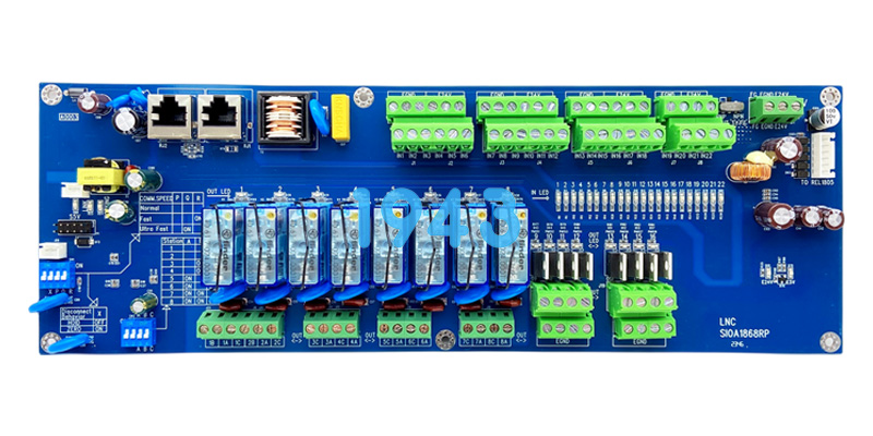
Achieving SMT Precision and Control in an HMLV Environment
The key differentiator between low-volume prototyping and high-volume production lies in line changeover frequency and setup complexity. SMT lines configured for high-mix production must reconfigure quickly while maintaining strict precision across diverse board designs and component inventories.
High-precision automated SMT equipment, supported by dual-head multi-feeder configurations, is necessary to handle a vast spectrum of component types, from 01005 passive components to large BGA packages or complex connectors.
Controlling solder deposition is a primary process gate. Automated three-dimensional Solder Paste Inspection (SPI) is mandatory for these applications. By measuring solder paste height, area, and volume on every single pad, SPI systems prevent common defects—such as solder bridging or insufficient solder—before components are placed, significantly improving yields.
Furthermore, advanced facilities often utilize nitrogen-purged reflow ovens. This environment minimizes oxidation on exposed copper pads and component leads, leading to improved solder wetting and more robust metallurgical bonds, particularly critical for complex multilayer boards and high-reliability components.
Validating the First Article and Closed-Loop Quality Control
Relying on post-assembly troubleshooting is not a viable strategy in HMLV manufacturing, where a single wasted component or project delay can be critical. Effective NPI requires a closed-loop quality framework focused on early defect detection.
A key component of this framework is Automated First Article Inspection (FAI). Before executing an entire pilot run, the first fully assembled assembly undergoes automated optical and electrical value testing.
The FAI machine verifies individual component values, tolerances, and placement alignment against the original CAD netlist and Bill of Materials. This automated verification eliminates human error and confirms that the SMT line is set up correctly and the correct component reels are loaded.
Post-reflow validation is then supported by integrated AOI and X-ray systems, which identify subtle defects such as BGA voiding or lifted leads that visual inspection cannot detect, providing actionable data to optimize process parameters.

Yield Optimization and the Path to Pilot Production
Once initial prototype functionality is validated, the focus of the NPI process transitions toward optimizing yield for the subsequent pilot manufacturing run (ranging from 50 to 1,000 units). This transition involves locking in critical process parameters, including SMT reflow temperature profiles, feeder assignments, and stencil printing specifications, to ensure total consistency across future builds.
A comprehensive DFM feedback loop is also formalized. Assembly technicians and quality engineers carefully document every manual intervention, layout anomaly, or thermal quirk encountered during the NPI phases.
This documentation is compiled into an actionable DFM feedback report, which is delivered back to the customer’s hardware engineering team. This process ensures that any manufacturing challenges are identified and resolved before the design is committed to larger-scale production.
FAQ Section: Small-Batch PCBA NPI
Q1: What is the typical lead time for a small-batch PCBA NPI prototype project?
A: For standard quick-turn NPI projects, prototype assembly can often be completed in 72 hours following DFM approval, depending on component availability and complexity.
Q2: How do you manage component sourcing for low-volume NPI runs to avoid minimum order quantity (MOQ) penalties?
A: We maintain an internal inventory of common passives and standard power ICs and leverage a network of franchised distributors globally. This enables us to source component quantities precisely required for small-batch runs, often utilizing cut-tape or mini-reel options to avoid MOQ penalties.
Q3: What panel size and design do you recommend for low-volume NPI runs?
A: We generally recommend standardized panels (e.g., 200mm x 250mm) featuring standardized rails (e.g., 5mm or 7mm) with 3mm tooling holes and optical fiducials. We work with clients to develop optimized panel layouts during the DFM phase.
Q4: Do you offer functional testing setup during the small-batch pilot run stage?
A: Yes. We work with customer-supplied test specifications, custom test fixtures, or 3D-printed enclosure jigs to execute comprehensive functional test routines, flash microcontrollers, and confirm operating voltage and signal levels on every unit prior to shipment.
Latest information
Let the products quickly and stably realize marketization and become the global electronic intelligence innovation enabler
 2026-11-06