
PCBA NPI for Industrial Automation: Prototyping to Pilot Runs
Managing Engineering Risk in Industrial PCBA Prototyping
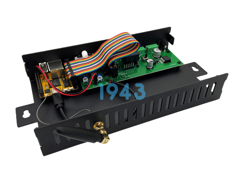
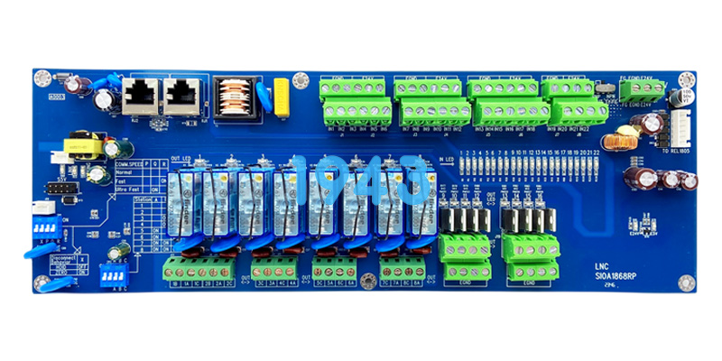
Industrial automation systems—such as programmable logic controllers (PLCs), motor drives, industrial gateways, and sensor hubs—operate under severe conditions. The transition from schematic capture to New Product Introduction (NPI) presents substantial engineering challenges, specifically regarding thermal performance, electrical integrity, and mechanical robustness. A malfunction during the pilot run phase directly compromises product certification paths and introduces costly delays to market entry.
Industrial PCBAs differ significantly from consumer products; they require sustained lifecycle support, compatibility with protective conformal coatings, tolerance for continuous mechanical vibration, and often utilize heavy copper layers to manage power requirements. Navigating the NPI cycle effectively demands a multi-pronged approach that includes rigorous Design for Manufacturability (DFM) analysis, proactively managing component lifecycle risks, and deploying a structured validation process from the initial prototypes to the pilot manufacturing run.
Technical DFM Priorities for High-Reliability Industrial Boards
Thermal management remains a primary technical hurdle. Industrial power supply and motor control boards frequently employ 2oz, 3oz, or thicker copper cladding on internal and external layers to satisfy high current density demands. However, these substantial copper planes function as massive heat sinks during the automated SMT reflow soldering process. They draw thermal energy away from component leads, which can lead to incomplete solder wetting, weak metallurgical bonds, cold solder joints, or defects such as tombstoning on passive components. To mitigate these risks, specialized multi-zone reflow profiles are requisite. These profiles necessitate extended soak times and carefully controlled ramp rates to ensure that multi-layer board structures with significant thermal mass achieve uniform thermal equilibrium without overheating sensitive surface-mount components or scorching thinner outer-layer laminates.
Mechanical stress management is equally critical. The continuous vibration and thermal cycling inherent in industrial installations dictate specific component footprint and assembly choices. Through-hole components, such as heavy terminal blocks or large capacitors, remain prevalent in industrial designs due to their superior mechanical strength compared to surface-mount equivalents. For these components, DFM reviews must ensure sufficient thermal relief areas on internal ground or power planes. This prevents the large copper masses from sinking heat too rapidly, ensuring adequate solder flow and full 180-degree vertical barrel fill during selective soldering or automated wave soldering processes. Failure to achieve proper solder fill can lead to mechanical connection failure over time.

Mitigating Component Obsolescence and Long Lead-Time ICs
Industrial equipment typically carries extensive product lifecycles, often spanning a decade or more. Consequently, component obsolescence is a persistent threat. Microcontrollers, industrial fieldbus transceivers, and specialized analog-to-digital converters regularly enter End-of-Life (EOL) or Product Change Notification (PCN) status well before the equipment's retirement.
Effective NPI requires aggressive Bill of Materials (BOM) scrubbing during the earliest stages. Prior to finalized design rule checks and bare-board fabrication, the BOM must be analyzed to identify any components flagged as Not Recommended for New Designs (NRND) or approaching EOL. Early identification allows engineering teams time to qualify pin-compatible alternate parts or revise the layout, avoiding critical component shortages or costly layout re-spins during the fabrication of the pilot production run.
Structuring the NPI Process Validation
The validation sequence during the NPI phase is designed to build confidence in both the design and the manufacturing process. It typically begins with a highly focused Engineering Prototype stage. This involves assembling a small quantity, perhaps 5 to 10 units, with the primary objective of verifying schematic logic, board layer stackup, component clearances, and basic power-up functionality. Following initial validation, First Article Inspection (FAI) is implemented.
Advanced manufacturing facilities utilize automated optical inspection and X-ray inspection to confirm solder joint integrity, particularly for bottom-termination components such as QFNs and BGAs where visual inspection is not possible. Finally, the process scales to the Pilot Production Run, which might range from 50 to 500 units. This phase is crucial for validating the repeatability of the automated SMT lines, the stability of the reflow profiles, the efficacy of functional test fixtures, and the board's performance under operational loads.

FAQ Section: Industrial PCBA NPI
Q1: How do you handle thermal profiles for multi-layer industrial PCBs with heavy ground planes?
A: We deploy customized multi-zone SMT reflow profiles. By extending the preheat and soak zones, the entire multi-layer assembly achieves uniform thermal distribution, preventing cold solder joints on high-thermal-mass ground pads while protecting sensitive ICs.
Q2: Can you assemble low-volume industrial boards with mixed SMT and through-hole technology?
A: Yes. We use automated SMT lines for surface-mount components combined with selective soldering or pin-in-paste reflow processes for through-hole connectors and heavy power components, eliminating the inconsistency inherent in manual soldering.
Q3: What documentation is required to initiate a DFM review for an industrial PCBA?
A: We require Gerber files (preferably in ODB++ format, though RS-274X is acceptable), an itemized Bill of Materials (BOM) including manufacturer part numbers, pick-and-place XY data, and fabrication drawings specifying dielectric stackup, copper weight, and desired surface finish.
Q4: How do you prevent BGA solder voiding on industrial communications boards?
A: We utilize X-Ray Inspection to monitor BGA voiding levels against IPC-A-610 Class 2 or Class 3 criteria. We optimize solder paste stencil aperture designs and strictly control reflow peak temperatures to ensure voiding remains well under specified thresholds.
Latest information
Let the products quickly and stably realize marketization and become the global electronic intelligence innovation enabler
 2026-11-06