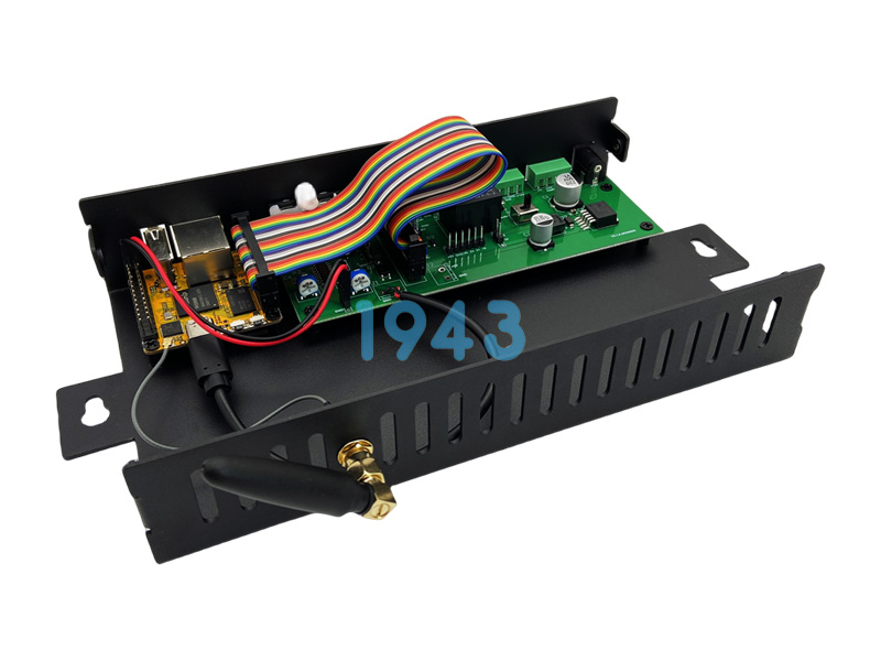

Design for Manufacturing Review in Low-Volume PCB Assembly
Design for manufacturing review, commonly called DFM review, is the first technical stage of a controlled PCBA NPI build. In low-volume PCB assembly, DFM review prevents the most expensive class of problems: those that appear only after boards are panelized, stencils are made, and components are placed. This article describes what a DFM review covers, what typical findings look like, and how the results affect later assembly and test stages.
Where DFM review fits in the NPI sequence
DFM review should happen before stencil fabrication and material ordering. Once solder paste stencils are cut or components are purchased in quantity, correcting a pad size or package mismatch creates cost and schedule delay. In a small-batch NPI workflow, the assembler reviews the design files and returns a report with recommended changes. The customer approves or rejects each item before the build proceeds.
The review is not a design verification review. It does not check whether the circuit functions as intended. It checks whether the board can be manufactured reliably with standard PCB assembly processes. The two activities are complementary, but they answer different questions.
File inputs for DFM review
A complete DFM review requires Gerber data, a bill of materials with manufacturer and part number, a centroid file, assembly drawings, and any special process notes. Missing data often forces assumptions that later prove incorrect. For example, if the centroid file does not include component rotation, the placement program may be built from the assembly drawing, which is slower and more prone to manual error.
The BOM should identify parts that are moisture-sensitive, static-sensitive, or temperature-limited. It should also indicate alternate parts if the primary source is not available. Without this information, the assembler may proceed with a part that fits the land pattern but cannot survive the reflow profile.

Common DFM findings in low-volume boards
Low-volume boards often have design features that are acceptable in a hand-built prototype but difficult in automated assembly. Common findings include missing fiducials, component spacing that leaves no room for rework, fine-pitch pads that are too wide or too narrow, and thermal relief patterns that cause tombstoning on small passives.
Fiducials are one of the most frequent omissions. A placement machine uses global and local fiducials to align the board and correct for panel stretch or individual board movement. Without fiducials, placement accuracy decreases, especially on boards with fine-pitch devices or large panel formats.
Component spacing affects both placement and rework. If a small capacitor is placed too close to a tall connector, the placement nozzle may collide with the connector during the placement of adjacent parts. If a BGA is surrounded by passives with no clearance, rework becomes difficult without disturbing nearby components.
Pad design also affects solder joint formation. A pad that extends too far under a QFN package can create solder bridging. A pad that is too small for a chip component may not form an adequate fillet. These issues can be corrected in CAD data before the first NPI run.
Solderability and surface finish considerations
DFM review includes a check of surface finish compatibility with the soldering process. ENIG, HASL, immersion silver, and OSP each behave differently in storage and reflow. For low-volume builds with a mix of large and small components, the selected finish affects wetting, flatness, and shelf life. The review does not recommend a finish in every case, but it identifies risks such as OSP exposure limits or uneven HASL thickness on fine-pitch pads.
Panelization and board outline
Boards that enter automated assembly must be panelized. The panel design determines how many boards fit in a standard frame, where tooling holes and fiducials are located, and how breakaway tabs are routed. A board without a clean breakaway path may require V-score or routed tabs that leave rough edges if not designed correctly.
DFM review checks the panel drawing against the assembly equipment. Components too close to the panel edge, overhanging connectors, or boards with uneven outlines may require special tooling. These details matter in low-volume production because custom pallets and fixtures add non-recurring cost that can be avoided with a simple CAD change.
Impact on stencil design and print quality
Stencil design is driven by DFM findings. Fine-pitch devices need smaller apertures and thinner stencil foil. Large power devices may need stepped stencil areas or solder paste deposit increases. If DFM review identifies a mixed-density board with both 0.4 mm pitch devices and large thermal pads, the stencil may require a step-up or step-down design rather than a uniform thickness.
Aperture wall quality, aspect ratio, and area ratio determine paste release. The DFM report often includes aperture recommendations for specific component types. For low-volume NPI runs, this is more practical than testing multiple stencil designs iteratively.

DFM review and testability
Test access is another DFM concern. The review checks for test points, probe clearance, and isolation of critical nodes. If the board will use flying probe or in-circuit test, test points must be accessible from at least one side and must not be covered by tall components or shields. If functional test requires connector access, the placement of connectors must allow the test fixture to mate without interference.
In low-volume boards, test access is often deprioritized because the first prototypes were tested manually. The DFM report brings these issues forward before the NPI run so that the test plan can match the board layout.
What a DFM report should include
A practical DFM report is itemized and traceable. Each finding should include a location, a description, a risk level, and a recommended action. Screenshots or Gerber views help when the issue is visual. The report should be short enough to review in one sitting but detailed enough that the design team can act without asking for clarification.
Shenzhen 1943 Technology Co., Ltd. performs DFM review as part of its small-batch PCBA NPI service. The review output is shared with the customer before material preparation, so design changes can be made while they are still inexpensive.

FAQ
1. What is the difference between DFM review and design rule check?
Design rule check verifies layout rules such as trace width and clearance. DFM review verifies whether the board can be assembled, soldered, inspected, and tested with available manufacturing equipment and processes.
2. What file formats are accepted for DFM review?
Typical inputs include Gerber RS-274X, ODB++, IPC-2581, or native CAD files if available. The BOM and centroid file must match the Gerber layer naming and component reference designators.
3. How long does a DFM review take for a low-volume PCBA project?
For a typical board with a few hundred components, an initial DFM report can usually be completed within one to three working days after receiving complete files. Incomplete or conflicting data adds review time.
4. Does Shenzhen 1943 Technology require DFM approval before starting an NPI build?
Yes. The build does not proceed until the customer reviews the DFM findings and confirms which items should be corrected or accepted. This prevents unapproved design changes from entering the manufacturing process.
Latest information
Let the products quickly and stably realize marketization and become the global electronic intelligence innovation enabler
 2026-11-06